Research Interests & Student Research Opportunities
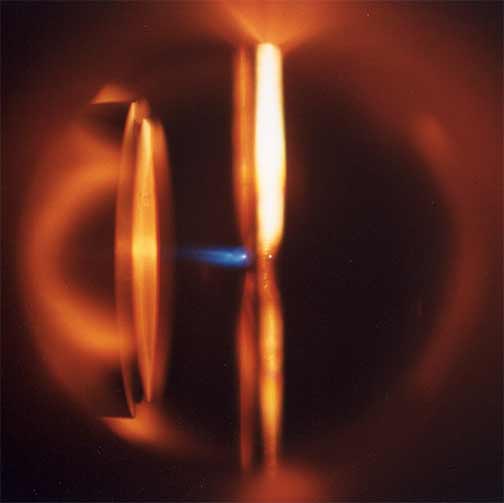
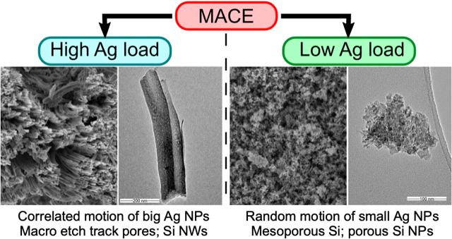
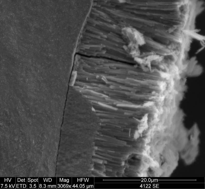
I like to make luminescent material and describe reaction dynamics. My research investigates dynamical processes at the surfaces of metals and semiconductors with a special emphasis on structure formation and laser-surface interactions. My co-workers and I are studying photochemical and thermal reactions on surfaces. Etching and growth to form nanoscale and larger structures are of particular interest. A great deal of my work has involved pointing lasers at or near surfaces and observing what happens. We use lasers to investigate what is occurring at the surface; to probe the properties of interfaces and porous materials; and to initiate chemical reactions and physical changes in interfaces and porous materials. The red image on the left is a photo I took of an ultrafast dye laser that I used at NIST. The scanning electron microscope (SEM) image in the middle is of a porosified silicon particle created by metal assisted catalyzed etching (MACE).The image on the right is of the nanosecond Nd:YAG laser we use for ablation at WCU.


Anodic and Electroless Etching of Si Wafers and Powders
K. Tamarov, J.D. Swanson, B.A. Unger, K.W. Kolasinski, T.A. Ernst, M. Aindow, V.-P. Lehto, J. Riikonen
Controlling the nature of etched Si nanostructures: High versus low load metal-assisted
catalytic etching (MACE) of Si powders. ACS Appl. Mater. Interfaces 12, 4787-4796 (2020).
.
E. Mäkilä, A.-M. Anton Willmore, H. Yu, M. Irri, M. Aindow, T. Teesalu, L. T. Canham, K. W. Kolasinski, J. Salonen
Hierarchical Nanostructuring of Porous Silicon with Electrochemical and Regenerative Electroless Etching, ACS Nano (2019).
C. Cozzi, G. Polito, K. W. Kolasinski, G. Barillaro
Controlled Microfabrication of High-Aspect-Ratio Structures in Silicon at the Highest Etching Rates: The Role of H2O2 in the Anodic Dissolution of Silicon in Acidic Electrolytes, Adv. Func. Mater. 2017.

J.A. DiPietro & K.W. Kolasinski,
Characterization of Mechanochemical Modification of Porous Silicon with Arginine. Surfaces 5, 143-154 (2022).
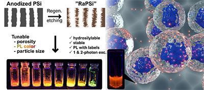
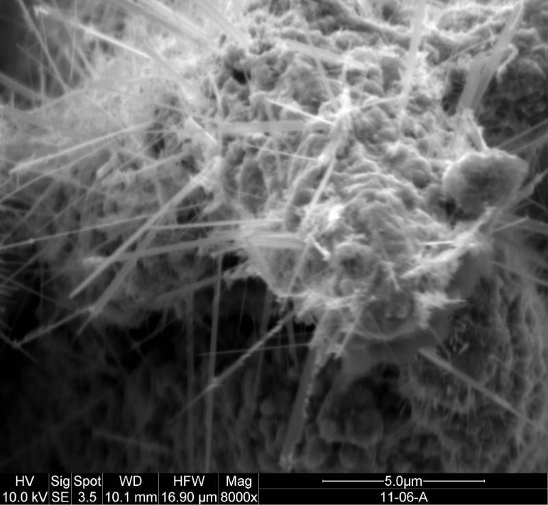
We investigate the formation of porous silicon by electroless methods, so-called stain etching. In stain etching an oxidant is mixed with fluoride to form an aqueous solution that spontaneously produces porous silicon once a silicon crystal has been dipped in it. We are now investigating the role of the oxidant and how it can be used to control both the photoluminescence spectrum and the morphology of the por-Si film. We have demonstrated that several ions work well, including Fe(III), Ce(IV) and IrCl62- and we now have a quantitative understanding of charge transfer in terms of Marcus theory. The V(V) ion has been used to form uniform films that can be as much as 20 µm thick. Our newly discovered ReEtching process allows us to form por-Si powder with fully etched particles as well as porous particles with hierarchical nanostructures. Now we are applying advances developed for ReEtching to metal assisted catalytic etching (MACE).
As described below, we make macroporous silicon (porous silicon with very large pores) by etching pillar-covered Si substrates in alkaline solutions.
Read more on porous silicon.
Irradiation with laser light fundamentally alters the surface chemistry of silicon. For instance, whereas clean crystalline Si is virtually inert to aqueous hydrofluoric acid, irradiation of a Si crystal immersed in HF(aq) with a cw visible laser can lead to the formation of porous Si. We are studying these processes in order to determine what factors affect the photochemical reactivity of Si surface and to develop a mechanistic understanding of the photochemical reactions involved. An example can be found here in J. Amer. Chem. Soc.
Laser Ablation Pillar Formation & Modification

Hexagonal macropore etched into pillar-covered Si crystal
Laser irradiation of semiconductors and metals, under the appropriate conditions can
lead to the spontaneous formation of conical structures. When made with a femtosecond laser, these pillars can be ten or so micrometers long.
The tips, however, are on the order of a few hundred nanometers or less. Using a nanosecond
laser, the pillars are much larger, up to 100 µm or more and a few micrometers at
their tip. We have shown that we can make such pillars in silicon, germanium as well as titanium and a number of other metals including Zn, Sn and Ni.
We have used alkaline solutions (concentrated KOH or tetramethylammonium hydroxide,
TMAH) to etch silicon pillars. Short etching times produce sharpened pillars. More
extensive etching creates crystallographically-defined macropores that are several
micrometers wide, such as the hexagon shown left, or macropore membranes.
Read more on pillars and macropores.
Read more on nanoparticle formation during laser ablation.
ZnO nanorods grown on a Zn laser ablation pillar
Anodic Titania Nanotubes & Porous Alumina
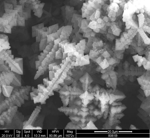
NH 4 AlF 4 nanoscepters
This project involves electrochemically etching Ti or Al to created arrays of nanotubes or pores while simultaneously oxidizing the metal to its oxide (titania, TiO 2, or alumina, Al 2 O 3 ). Read more about anodic titania nanotubes.
TiO 2 nanotubes
Dynamics of Adsorption and Desorption
I have long studied the simplest of surface chemical reactions, the adsorption and thermal desorption of small molecules from surfaces, particularly hydrogen on silicon. I have also reviewed stimulated desorption of hydrogen from silicon. While this work has laid the foundation for much of my research, currently these are not the types of studies that I'm performing in my lab in West Chester. Rather they are part of what of do when I work with, for instance, Eckart Hasselbrink in Essen, Germany.
Solidification Driven Extrusion (Nanospikes)
While making silicon and germanium pillars, we noticed that nanoscale spikes form atop the pillars. We subsequently showed that the same physics that is behind this phenomenon is also active in your freezer and can result in the formation of centimeter long ice spikes.
Solidification Driven Extrusion (Nanospikes)
Dave Mills, who now spends some of his time reading old scrolls with X-rays, noted
that in some of the scanning electron microscopy (SEM) images that he took of our
laser ablation created silicon pillars, that a little spike formed on the tip of the pillar. He also thought that these
might be related to ice spikes. You can get ice spikes to form in your freezer simply by freezing pure distilled
water. A major question in nanoscience is: what techniques to form structures scale
from the macroscopic (for instance centimeter) range into the nanoscale regime? We
showed that the physics behind ice spike formation scales down to the nanoscale. It works
for silicon pillars just like it works for ice cubes.
In subsequent work with germanium performed with Barada Nayak and Mool Gupta, we found that nanospikes
also form on germanium pillars, as shown on the right.
So what do water, silicon and germanium all have in common? They all form tetrahedrally
co-ordinated solids phases and all of them expand when they freeze. This is an unusual
property but that is what makes ice less dense than liquid water and why ice cubes
float. It also means that if the surface of liquid water, silicon or germanium freezes
that it compresses the liquid that is trapped inside. This leads to a build up of
pressure. Eventually the pressure is too much and a jet of supercooled liquid shoots
out and forms the ice spike.
Ultrafast Surface Photochemistry in the VUV
This was a project I worked on while at the University of Birmingham that involves the use of femtosecond pulsed lasers to create vacuum ultraviolet photons via high harmonic generation.
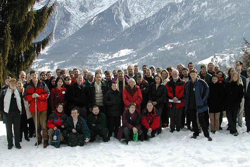
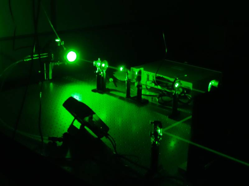
This project was part of a TMR Network. Being part of a TMR network is often hard work, including walking up snowy mountain roads and skiing. During this work, we built a rather unique machine to study ultrafast (about 1 ps or less) photochemistry in the vacuum ultraviolet regime. A schematic drawing of the apparatus appears below. The required photons were made through a laser-based technique: high harmonic generation with an Ar-ion-pumped Ti:sapphire laser. This laser produces roughly 80 fs pulses at a wavelength near 800 nm. The output of the Ti:sapphire laser is focused into a rare gas that flows out of a tube in a vacuum chamber, as shown in the photo on the right. A nonlinear interaction between the laser field and the atoms in the rare gas jet creates the photons that we are after: ~10-40 eV or 120-30 nm. We studied the photochemistry of O2 adsorbed on graphite. This was the first use of HHG to initiate surface photochemistry.