
Photochemical & Chemical Modification of Si and Porous Si
Porous silicon is silicon with lots of holes in it and has properties that are much different than that of bulk crystalline or polycrystalline silicon. There is great interest in obtaining light from nanoscale Si [see links ( 1 ), (2) and (3)] structures for optoelectronic, nanoelectronic and biomedical applications, even fuel cells. I've been very interested in several aspects of porous silicon formation including the mechanism by which HF attacks the silicon and how etching conditions affect the optical and structural properties of the resulting thin film. We done work on the mechanism of etching, the photoluminescence of porous silicon, the structure of the film after laser-assisted etching or stain etching, deposition of other photoluminescent material during etching, and new methods to measure etch rates and porosity. To understand etching in acidic fluoride solutions it is also important to consider the nature of the highlynon-ideal fluoride solutions and their composition.
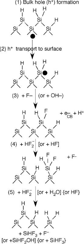
HF (hydrofluoric acid) is rather unreactive with a silicon surface because once it removes any oxide layers, it leaves the surface hydrogen terminated with one H atom bound to each surface Si atom. To initiate further reactivity and etching this H-terminated surface has to be activated in one of three ways: (i) electrochemically by applying a sufficient voltage (anodic etching), (ii) electrochemically by adding an oxidant with a sufficient standard electrode potential (stain etching), or (iii) photoelectrochemically by irradiating the silicon with a laser or lamp with a sufficiently short wavelength to excited electrons to the conduction band. In all three cases, a vacancy is formed in the silicon valence band. A vacancy is also called a hole. In other words, an electron is removed from near one of the Si–H bonds. This activates the previously passivated Si–H bond, making it susceptible to attack by the fluoride solution. After initiation, the etching of one silicon atom proceeds very rapidly according to the mechanism outlined to the right.
We've also investigated reactions that occur either during or after porous silicon formation. Etching results in the formation of the hexafluorosilicate anion, (SiF6)2–. When etching is performed in the presence of cations that create an insoluble salt such as K+, Rb+ and Cs+, a hexafluorosilicate salt can precipitate out on the porous silicon surface. When such a layer is irradiated with ultraviolet light, the layer emits light. This process is called photoluminescence. After a porous silicon layer is formed it is initially H-terminated. Irradiation of porous silicon with an ultrafast 120 fs duration infrared laser pulse in the presence of ethanol leads to a reaction between the por-Si surface and the ethanol. The attachment of ethanol to the porous silicon changes the optical properties of the por-Si layer. The photoluminescence goes away but the reacted thin film is very efficient at facilitating the combination of two ultrafast infrared photons into a new visible photon - a process known as sum frequency generation
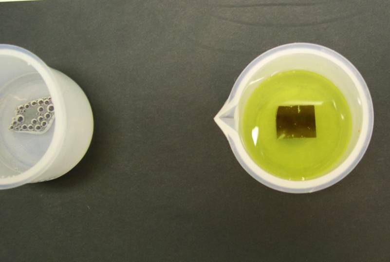
Above you see a photo of porous silicon being made by stain etching. On the left is a "conventional" stain etchant made from HNO3 + HF. On the right is an improved stain etchant made of Fe(III) + HF. The colors on the Si surface are produced by white light interference effects. The uniformity of the film and the flattness of its upper and lower interfaces are indicated by the uniformity of color. We've been workiing hard to make films more uniform. We need to avoid the formation of bubbles. Bubbles cause problems in that they cover the surface. This blocks access to the surface by the solution and results in inhomogeneities in the porous thin film. An etchant that uses Fe(III) as an oxidant does a good job of doing this, particularly if the concentration of Fe(III) is low. We have recently discovered two new oxidants (V in the +5 oxidation state and Ce in the +4 oxidation state) that are even better. In fact, Vesta Ceramics uses a process developed by us to form porous silicon powder.
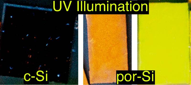
To make microporous (also sometimes called nanoporous) photoluminescent porous silicon
we primarily use stain etching. In the image to the left above you can see that bulk crystalline Si does not exhibit
visible photoluminescence when illuminated with UV light but that stain etched Si
is a brilliant emitter of visible light in the green to red range. In stain etching
an oxidant is mixed with fluoride to form an aqueous solution that spontaneously produces
porous silicon once a silicon crystal has been dipped in it. We have already shown
that the fluoride can be provided not only by HF but also by NH4HF2.
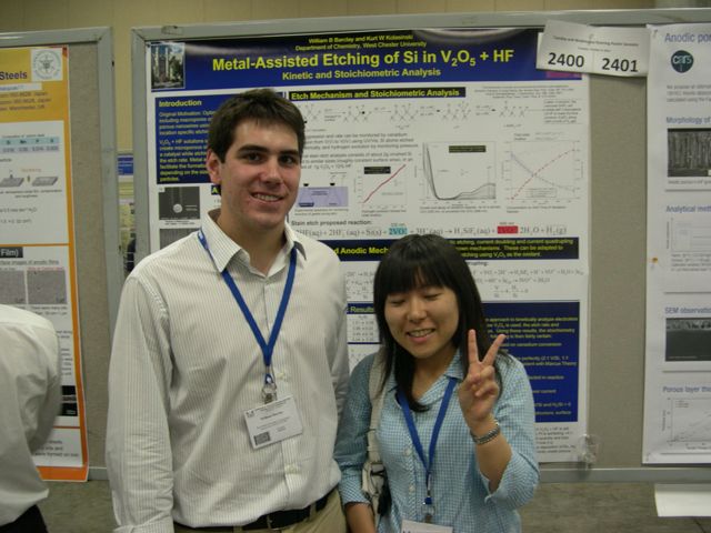
Brett Barclay, here with a colleague from Japan, reported on some of our stain etching results at the Electrochemical Society meeting in Honolulu, Hawai'i.
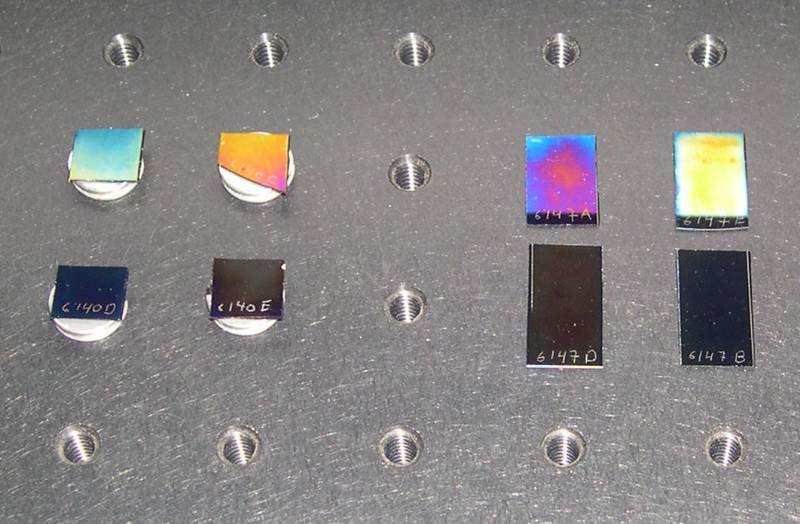
At WCU we've been investigating the role of different types of oxidants. Maggie Dudley, who won the College of Arts & Sciences Outstanding Student Award in 2008, was involved on the initials studies with the Fe(III) and V(V) ions. We've also shown that Ce(IV) acts as an effective oxidant.
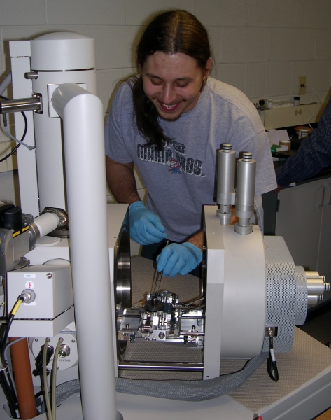
Bryan Kelly, pictured, inserting a sample into the scanning electron microscopy (SEM) for structural and elemental analysis.
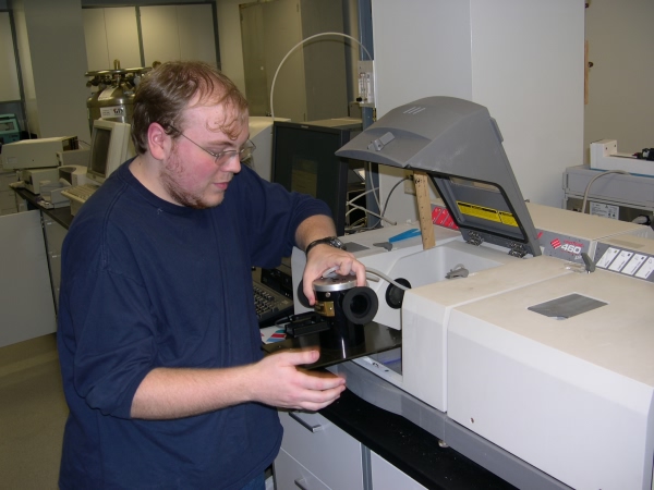
Justin Hartline, pictured, working with the Fourier transform infrared (FTIR) spectrometer, followed up on these studies and helped to develop a new method of probing the films with FTIR spectroscopy.
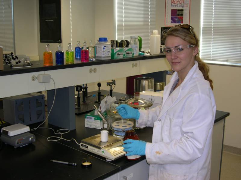
Julia Yadlovskiy performed extensive experiments to investigate the V2O5 + HF stain etchant. These studies examined the kinetics of film formation. The effects of the V2O5 concentration, HF concentration and addition of ethanol and acetic acid were all studied.

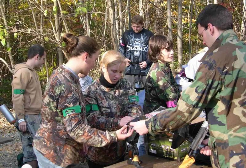
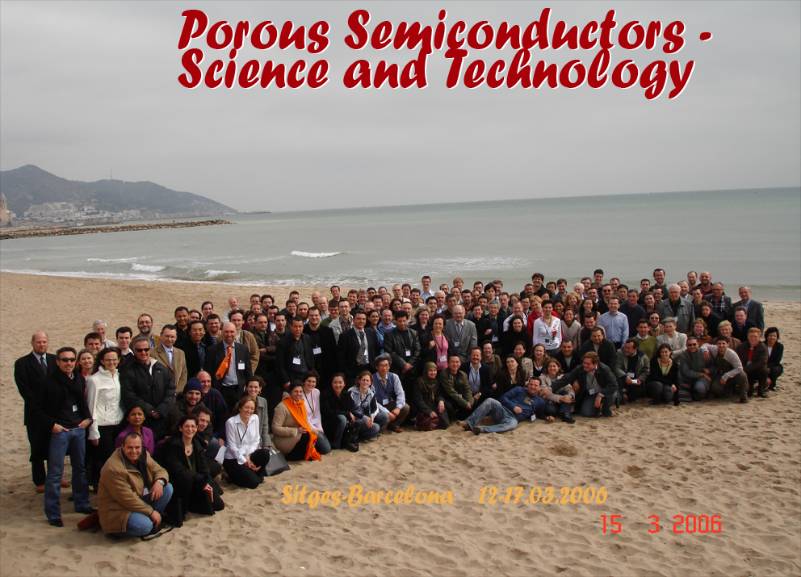
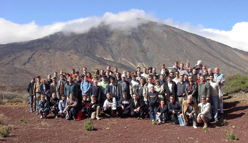
Working with porous silicon has its advantages. Not only is there a lively community of researchers in the field but we also like to meet at the beach in Tenerife or Catalonia or sometimes on a volcano such as El Teide in Tenerife. In the tradition of "porous silicon researchers only have their photos taken outdoors," Maggie steadfastly refused to have a lab photo taken but I did manage to get a photo during paintball. For which she repaid me by shooting me between the eyes.
For further information on related topics, try these sites:
- Labs working in Surface Science, Nanotechnology and Catalysis
- Porous Semiconductors Science & Technology
- Optoelectronics with porous silicon at Univ of Bath Centre for Photonics and Photonic Materials
- Sailor Research Group and an introduction to porous silicon
- Biosilicon from pSivida